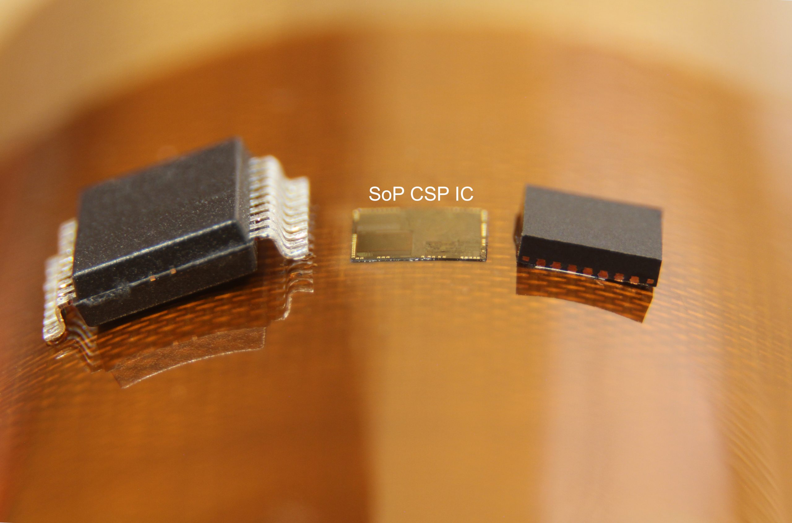
Semiconductor-on-Polymer™ Chip Scale Packaging
Semiconductor-on-Polymer (SoP™) Protected-WLCSP, aka P-WLCSP, is an advanced CSP process for 200mm and 300mm wafers. The FleX-C SoP process can be used to protect two sides of the die. The SoP-TM process can fully encase all six sides (6s) of the die. Either process can be applied to bulk or SOI wafers from any Foundry or IDM.
SoP is a thin-device process. Silicon thickness are supported from 100um to 0.2um and can be tailored to customer requirements. 10um silicon is often considered “standard” for this technology due to its proven capability to bend and has been useful for applications that require curved surface conformity or flexibility. 100um versions of the SoP processes are available if needed for current assembly flows and provide an excellent starting point with a proven path to ultra-thin when needed.
American Semiconductor can provide SoP P-WLCSP processing to very small lots for qualification. In some cases, SoP processing can be provided for MPW wafers from foundries such as Tower Semiconductor and TSMC.
Technology details for SoP are provided on the Resources page.
For more information on packaging your die in SoP, contact sales@americansemi.com for wafer requirements and pricing.